sábado, 24 de julio de 2010

Simulations cast light on CIGS solar cell efficiency puzzle

Computer simulations of copper indium gallium diselenide alloy (CuInxGa1-xSe2, or CIGS) suggest that indium segregation effects may play an important role in reducing the conversion efficiencies of photovoltaic/solar cell devices based on the material [Christian D. R. Ludwig et al, Physical Review Letters, vol105, p025702, 2010].

Despite these problems, the best CIGS solar cells have achieved efficiencies of 20.1%, although commercial devices fall somewhat short of this (up to ~14%). The theoretical maximum is around 30%. CIGS is one of the leading contenders for low-cost production of relatively high-efficiency cells.

The calculations were carried out by researchers at Johannes Gutenberg-Universität Mainz, IBM and Universität Duisburg-Essen. In fact, the lead author of the paper, Christian Ludwig, used a mainframe for his investigations that was recently donated to Mainz University by IBM as part of a Shared University Research (SUR) science award.

The starting point for the study was the observation that, despite an optimal bandgap for solar radiation absorption suggesting that a CIGS material with 70% Ga should yield the highest efficiency, in fact 30% Ga is experimentally found to be best. The estimate is based on the bandgaps of the non-alloyed materials CuInSe2 (1.0eV) and CuGaSe2 (1.7eV).

Indium segregation is a common problem for nitride semiconductors used to create green-blue-violet-ultraviolet light-emitting devices. Indium segregation refers to variations in the balance of indium and the other group III materials (such as gallium) in the alloy material.

The effect of indium segregation is not always negative – in some nitride light-emitting devices it is thought that the segregation effect creates localized states that can boost emission efficiencies in some cases. However, in the case of solar cells such effects are almost certainly detrimental, particularly in leading to fluctuations in the material’s bandgap energy value.

The simulations used a hybrid of density functional theory (DFT), cluster expansion and Monte Carlo methods to simulate larger samples than usual with pure DFT. The cluster expansion is used to extract interaction energies from the DFT results that are used in the Monte Carlo of larger systems.

Dr Thomas Gruhn, head of the theory group involved in the work, explains the methods used: “Density functional calculations make it possible to assess the energies of local structures from the quantum mechanical point of view. The results can be used to determine temperature effects over wide length-scale ranges with the help of Monte Carlo simulations.”


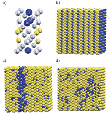
Figure 1. (a) CIGS unit cells showing positions of atoms in series of unit cells. Snapshots of: (b) a system of periodic unit cells; (c) the Ga-rich system at 348K; (d) the Ga-rich system at 406K (Ga atoms are yellow; In atoms are blue). Cu and Se are not displayed in the snapshots, and the size of the spheres is arbitrary.

The calculations ignore possible defects of the Cu and Se atom sites, concentrating on the effects of variations in the Ga/In site occupation in the crystal structure (Figure 1a). The formation energies of 32 CIGS structures were calculated using DFT methods. The Monte Carlo used supercells with up to 32 atoms with a simulation box measuring 16x16x8 (8192) active atoms. The temperature range of the simulations was between 290K (room temperature-ish) and typical CIGS process temperatures of 870K. The resulting inhomogeneity was assessed using cubic segments consisting of 16 atom sites. The standard deviation was used as a measure of inhomogeneity.

Two alloy systems were studied: ‘Ga-rich’ CuIn0.25Ga0.75Se2 and ‘In-rich’ CuIn0.75Ga0.25Se2. At low temperatures (290K) a histogram of the segment compositions show two peaks — one being around a few atoms of the non-rich atom, the other a small peak for the non-rich atom at around 15 (Figure 2). This is an indication of segregation with regions of unalloyed material — CuInSe2 (CIS) and CuGaSe2 (CGS). At higher temperatures, this behavior decreases and the alloy becomes more homogeneous.


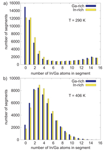
Figure 2. Histograms showing number of cubic segments in simulation box that contain 1–16 atoms of a certain type. Blue is the distribution of In atoms in Ga-rich CIGS, and yellow is the distribution of Ga atoms in In-rich CIGS at temperatures of (a) 290K and (b) 406K. A perfectly ordered In-rich or Ga-rich system would have 4 Ga/In atoms in every segment – the histogram would then have all entries in bin 4.

The segregation effect at low temperature is found to be worse for Ga-rich material, perhaps explaining the poorer performance of 70% Ga compared with 30% Ga CIGS solar cells. The mean value for both types is 4 non-rich atoms per box. The standard deviation is always higher for Ga-rich CIGS, again indicating higher inhomogeneity.

These results suggest that fast cooling of high-temperature processed material could minimize bandgap fluctuations, leading to better solar cell performance. The authors comment: “The lack of phase separation in actual solar cells shows that the In-Ga distribution is ‘frozen’ in a high-temperature state. Thus, higher production temperatures and a reasonably fast cooling will lead to better efficiencies, which has recently been shown experimentally.”

In practice, such fast cooling has been limited by the heat resistance of the glass used as a substrate for CIGS solar cells.

This research forms part of the comCIGS project, which is looking to optimize CIGS solar cells with funding from the Federal German Ministry for the Environment, Nature Conservation, and Nuclear Safety (BMU). The project involves IBM Mainz and Schott AG, along with Johannes Gutenberg-Universität Mainz, the Helmholtz Center Berlin for Materials and Energy and Jena University.

To enable faster cooling of CIGS solar cells, Schott AG has developed a special glass with which the process temperature can be increased to well above 600°C. The cells that result are considerably more homogeneous, opening the way to cells with greater efficiency levels.

Gruhn reports: “We are currently working on large-format solar cells which should outperform conventional cells in terms of efficiency.”

Fuente: http://www.semiconductor-today.com/news_items/2010/JULY/MAINZ_220710.html

Mario Pedraza
Electrónica del Estado Sólido
Sección 2

Unos revolucionarios cristales guardan mil millones de gigas

Científicos norteamericanos han descubierto un material que es capaz de almacenar entre mil y un millón de veces más datos que las actuales memorias de hoy. Esta capacidad de albergar información no tiene precedentes y en no demasiado tiempo podríamos estar hablando de chips de memoria de 1 Exabyte, mil millones de gigas. Espectacular avance que llevará a la informática a cotas nunca vistas. La singularidad tecnológica se acerca.

Los cristales pueden albergar una cantidad de información nunca vista hasta ahora.

Los investigadores de la Universidad de Florida trabajan en unos exóticos materiales que serán capaces de almacenar una cantidad de información nunca vista hasta ahora. Dicen los responsables del estudio que se trata de unos cristales muy particulares que funcionan de una manera determinada en el ámbito químico, de tal modo que los cristales ya poseen una estructura especial a nivel nanométrico que les permite guardar los datos de forma inherente. Normalmente los chips se fabrican pensando en interponer capas de material que se pueda interpretar como valores almacenados, pero estos extraños cristales lo hacen de modo natural gracias a sus particulares estructuras atómicas.

Naresh S. Dalal, el experto en bioquímica que se encarga de la investigación, dice que son «materiales multiferroicos» y eso quiere decir que son al mismo tiempo ferromagnéticos y ferroeléctricos, dependiendo de la temperatura a que sean sometidos. «Normalmente, estas dos propiedades son mutuamente excluyentes», dijo Dalal. «La mayoría de los materiales son ferromagnéticos o ferroeléctricos y están basados en el número de electrones en la capa electrónica exterior del ion. Por lo tanto, la búsqueda de cuatro materiales multiferroicos al mismo tiempo es científicamente significativo y abre numerosas puertas en términos de aplicaciones potenciales».

En teoría, con esos cuatro cristales se podrían diseñar chips mucho más pequeños y mucho más capaces en cuanto al almacenamiento de datos. Del orden de un millón de veces. Mientras que una tarjeta SD actual guarda 1 Gigabyte, un dispositivo del mismo tamaño hecho con estos materiales podría albergar hasta 1 Exabyte. La mala noticia es que, por ahora, esos exóticos cristales necesitan estar a 150 grados bajo cero para funcionar con esas capacidades. Se está estudiando para ver si se encuentran materiales similares a temperatura ambiente. Tu ludoteca universal tendrá que esperar otros tantos años o, en todo caso, comprarte un refrigerador de los buenos.

Fuente: http://www.abc.es/20100305/ciencia-tecnologia-tecnologia/cristales-guardan-millon-veces-201003051105.html

Mario Pedraza
Electrónica del Estado Sólido
Sección 2


viernes, 23 de julio de 2010

Puntos Cuánticos

Los puntos cuánticos (qdots o quantum dots en inglés) o átomos artificiales son nanoestructuras creadas en el laboratorio que miden millonésimas de milímetro —nanómetros—. Inventadas hace casi dos décadas, tienen un sinfín de aplicaciones en áreas tan variadas como las telecomunicaciones, la computación cuántica, la seguridad o la biomedicina.

En el mundo macroscópico, los puntos cuánticos pueden tener el aspecto de una simple pastilla plana, o estar disueltos en un líquido. Nadie sospecharía que esa sustancia ha sido construida en el laboratorio partiendo de unos pocos átomos, con técnicas que manipulan la materia a escalas de nanómetros. A esas dimensiones el material se convierte en una matriz sobre la que han crecido estructuras, como pirámides o montañas, formadas por unos pocos cientos o miles de átomos. Esas estructuras son los puntos cuánticos.

Lo especial es que, en ellos, los electrones están obligados a permanecer atrapados, confinados en las tres dimensiones, y eso genera curiosos fenómenos cuánticos. En concreto, los electrones se disponen en el punto como en un único átomo, de ahí el apodo átomos artificiales. Y de ahí, también, el que la materia estructurada en puntos cuánticos tenga propiedades que pueden ser controladas a voluntad.

Una de ellas es que, al ser iluminados, los puntos cuánticos reemiten luz en una longitud de onda muy específica y que depende del tamaño del punto cuántico. Cuanto más pequeños sean los puntos, menor es la longitud de onda y más acusadas las propiedades cuánticas de la luz que emiten. El resultado es que "puedes diseñar de antemano un punto cuántico para la longitud de onda que desees", explica Carlos Tejedor, del Departamento de Física Teórica de la Materia Condensada de la Universidad Autónoma de Madrid (UAM).

Esta una propiedad que los laboratorios llevan queriendo aprovechar desde principios de los noventa, "pero sólo ahora la tecnología de fabricación ha alcanzado un grado de calidad aceptable para las aplicaciones comerciales", señala Tejedor. "Ahora, el campo está en pleno auge". Fernando Briones, del Centro Nacional de Microelectrónica (CNM), del CSIC, lo corrobora: "Sí, últimamente hay ya una variada fauna de puntos cuánticos. Los hay de muchos tipos, para aplicaciones muy diferentes".

Un informe de este año de la compañía Business Communications Company aseguraba que para el 2009, el mercado global de puntos cuánticos, contando todas las aplicaciones, superaría los 500 millones de dólares (unos 400,64 millones de euros). Hay una aplicación obvia: la optoelectrónica. Con los puntos cuánticos de materiales semiconductores, como arseniuro de indio y fosfuro de indio, se fabrican diodos láser emisores de luz más eficientes que los usados hoy en lectores de CD, de códigos de barras y demás. Así que se espera que acaben sustituyéndolos a corto o medio plazo.

Pero además se abren muchas más posibilidades: en células fotovoltaicas, en telecomunicaciones, en seguridad —en billetes o documentos, en los que se embeben puntos cuánticos invisibles a simple vista—, en criptografía cuántica, o en computación cuántica, en la que los puntos cuánticos proporcionarían las unidades de información, los qubits, de los aún hipotéticos ordenadores cuánticos de enorme capacidad de cálculo. El año pasado, dos grupos consiguieron demostrar independientemente que es posible crear un vínculo cuántico —un entrelazamiento— entre dos puntos cuánticos, de forma que lo que le ocurra al uno afecte al otro y viceversa, un principio básico de los ordenadores cuánticos.

La investigación con puntos cuánticos en la UAM y en el CNM se orienta a su uso como componentes materiales para la información cuántica. Los grupos de Luisa González, Jorge García y Fernando Briones en el CNM fabrican ya diodos láser de altas prestaciones en los que se integran puntos cuánticos de semiconductor con técnicas de autoensamblado por epitaxia de haces moleculares.

Sin embargo, las aplicaciones que parecen llevar la delantera en cuanto a comercialización son las de biomedicina. En este caso, los puntos cuánticos no están embebidos en una matriz, sino que son cristales independientes, pero su fundamento y sus propiedades físicas son las mismas. Xavier Michelet, de la Universidad de California, coautor de una revisión sobre usos de puntos cuánticos en biología publicada en Science, explica por correo electrónico: "Los puntos cuánticos emiten luz brillante y muy estable. Con ellos se obtienen imágenes de mucho contraste usando láseres menos potentes, y no existe el temor de que se apaguen". Además, la longitud de onda tan específica a la que brillan evita las superposiciones, y permite teñir a la vez muchas más estructuras que con los métodos de tinción tradicionales.

El primer uso de los puntos cuánticos en biología fue en un embrión de rana, hace tres años. Los investigadores envolvieron los puntos cuánticos en micelas —moléculas que forman esferas solubles en agua— para poderlos sumergir en un medio húmedo, e inyectaron miles de millones de ellos en embriones de rana; después, con técnicas de imagen en vivo pudieron seguir a las células fluorescentes y a sus descendientes a medida que se iban diferenciando, durante varios días. En 2003, otro grupo obtuvo imágenes de los capilares de un ratón vivo al que se le habían inyectado los puntos cuánticos bajo la piel. Las imágenes tenían mil veces más resolución que las obtenidas con técnicas convencionales, hasta el punto de que se detectaba la vibración de los capilares al ritmo de los latidos cardiacos.

Pero, además, a los puntos cuánticos, que tienen más o menos el tamaño de las proteínas, se les puede pegar anticuerpos capaces de reconocer compuestos, células o virus. Muchos investigadores planean usarlos como marcadores de células cancerosas, a las que se podría seguir a medida que se multiplican o migran. Varios grupos han logrado ya que se adhieran a proteínas que flotan en la membrana de la célula —receptores—. Por ejemplo, el año pasado un grupo los usó para señalar la localización de nódulos linfáticos durante la propia operación para eliminarlos —en cerdos y ratones—. Y en abril de este año se publicó el uso de puntos cuánticos para detectar el virus respiratorio sincitial apenas una hora después de que infectara a células. También han sido usados en plantas, adheridos a una proteína que a su vez se pega al polen.

¿Se podrían, además, usar los puntos cuánticos como transportadores de fármacos hasta células específicas, por ejemplo? Responde Michelet: "La idea de los nanorrobots patrullando por la sangre es seductora (o temible, según el punto de vista), pero aún está lejos del estado actual del arte en nanotecnología. Sin embargo, hace tiempo que se piensa en una sonda molecular multimodal y los puntos cuánticos sí que pueden ser equipados con funciones suplementarias. Nosotros ya estamos haciendo algo así, poniendo en cada punto cuántico unos pocos péptidos con propiedades de solubilización; otros, para evitar que el punto cuántico se adhiera con otros tejidos; otros, para llegar al objetivo deseado... La lista de posibles añadidos al punto cuántico es interminable, y se les podría añadir moléculas con acción terapéutica".

Otra posibilidad ante la que los biólogos se frotan las manos es la de usar los puntos cuánticos como sondas moleculares que penetren dentro de la célula. Sería un campo del todo nuevo. En la tinción de células en vivo ya hay métodos muy buenos y, por tanto, los puntos cuánticos son una mejora o un método complementario, pero nunca antes se ha aspirado a "marcar unas pocas proteínas, cada una con su punto cuántico, y observarlas en el microscopio mientras realizan sus tareas en la célula", señala Michelet. "Sería como tener una cámara en miniatura dentro de la célula, un gran paso para la biología celular". Hasta ahora, sin embargo, los intentos en esta dirección no han dado buenos resultados porque la mayoría de las veces los puntos cuánticos acaban "en la maquinaria de reciclado de la célula", pero Michelet cree que es cuestión de tiempo.

Pero antes hay que resolver una cuestión clave: la toxicidad. Los puntos cuánticos usados en biología se hacen con cadmio y otros elementos tóxicos, pero eso no implica necesariamente que los puntos cuánticos deban serlo. "No hay datos aún para estimar la toxicidad de los nanocristales", escribían en Nature Biotechnology los autores del marcaje de los nódulos linfáticos. Recabar estos datos no es nada fácil debido a la gran diversidad de puntos cuánticos sintetizados por laboratorios que usan métodos y materiales distintos. Los institutos nacionales de salud estadounidenses han creado un Laboratorio de Caracterización en Nanotecnología que probará las muestras que envíen los grupos y decidirá si cumplen las normas de toxicidad establecidas por la Food and Drug Administration (FDA) de los Estados Unidos.

Fuente: http://axxon.com.ar/not/154/c-1540078.htm

Mario Pedraza
Electrónica del Estado Sólido
Sección 2

Paneles solares y móviles comenzarán a ser fabricados con grafeno en 2011

Resistente, flexible y de gran conductividad. Con propiedades entre semiconductor y metal, el grafeno es el material más resistente jamás descubierto y en el que los electrones se mueven con mayor facilidad, al menos cien veces más rápido que en el silicio. Sin embargo, esta forma de carbono puro de una sola capa atómica de espesor, que revolucionará la electrónica, la informática y las comunicaciones era difícil de producir a gran escala sin perder calidad.

Ya no lo es. Un grupo de investigadores de Samsung y de la universidad Sungkyunkwan, en Corea del Sur, han conseguido fabricar láminas flexibles de grafeno de 30 pulgadas (unos 76 centímetros de diagonal).

"El objetivo es utilizar una técnica muy parecida a la que se emplea para imprimir los periódicos, donde millones de páginas son impresas en muy poco tiempo. En este caso, en lugar de papel se usan rollos de un material plástico flexible y, en lugar de tinta, se deposita una capa de grafeno de bajo coste, que se utilizará en un futuro muy cercano como uno de los principales componentes de teléfonos móviles, televisores, paneles solares....", explica Tomás Palacios.

El equipo de investigación del Instituto Tecnológico de Massachussets (MIT), que lidera este ingeniero de telecomunicaciones español, es pionero en el desarrollo de circuitos y dispositivos electrónicos de grafeno. Su prototipo de transistor de grafeno de bajo coste fue presentado en la reunión anual de la Sociedad Americana de Física en marzo de 2009 y, desde entonces, "se han producido avances importantes y prometedores. Por ejemplo, IBM ha logrado fabricar transistores de grafeno funcionando a 100 gigahercios (100 GHz)".

Si se conectara al multiplicador de frecuencia de grafeno, también desarrollado por Palacios en 2009, "la frecuencia de la señal de salida se duplicaría".

La progresión de este material de propiedades únicas, que también está cambiando la manera en la que se estudia la física, es "increíble. Está pasando de ser un material muy interesante para la ciencia básica a tener claras aplicaciones industriales. Paneles solares y teléfonos móviles ya serán fabricados con grafeno el año que viene", considera Palacios.

En septiembre, el MIT inaugura el Centro de Investigación sobre el Grafeno, que lidera el ingeniero español. Un centro en que investigadores y empresas (entre ellas algunos de los grandes fabricantes de semiconductores) no sólo intercambiarán sus conocimientos; los llevarán a la práctica.

Paralelamente, su equipo en el MIT sigue investigando. Por un lado, ha fabricado con este material la radio más pequeña del mundo, "que permite escuchar cualquier emisora y ser conectada a un altavoz". Por otro, ha abierto una línea de investigación que mezcla la electrónica basada en grafeno con la biología. Se trata de un sensor sobre el que se depositan células vivas. Como éstas se comunican mediante impulsos eléctricos y químicos, "utilizamos el grafeno para medir dichos impulsos y estudiar cómo estas células se relacionan entre sí".

Análisis celular

El objetivo es desarrollar nuevos instrumentos no intrusivos para el estudio celular. Hasta ahora, médicos y biólogos sólo podían observar las células bajo el microscopio o pincharlas para medir su voltaje. "Con este nuevo instrumento se logra obtener la misma información, pero sin dañar la célula. Como este material sólo tiene un átomo de espesor, cualquier cambio que se produce en la célula (composición química, voltaje...) depositada sobre el sensor modifica la conductividad del grafeno", precisa Palacios.

Y añade: "Saber cómo éstas se comunican, es el primer paso para entender el funcionamiento de órganos como el cerebro y cómo las celulas responden ante medicamentos y enfermedades".

Complemento del Silicio

Pese a las únicas características del grafeno (resistencia, flexibilidad y gran conductividad) este material con propiedades entre semiconductor y metal no sustituirá al silicio, el segundo elemento más abundante en la corteza terrestre, que se obtiene de la arena y con el que se fabrican los chips desde mediados del siglo pasado. "Ambos son complementarios", sostiene Tomás Palacios.

Y se podrán combinar. Por ejemplo, "a un chip de silicio se le podría añadir un sensor de grafeno para medir la calidad del aire o capturar imágenes nocturnas". El grafeno también podría sustituir al cobre -y otros materiales- que conectan a los transistores de silicio dentro de un microprocesador. "El grafeno tiene menos resistencia eléctrica que el cobre y, por lo tanto, los microchips se calentarían menos". Este es uno de los principales escollos que impiden fabricar chips cada vez más pequeños a mayor frecuencia.

Fuente: http://www.elpais.com/articulo/portada/Paneles/solares/moviles/comenzaran/ser/fabricados/grafeno/2011/elpepisupcib/20100701elpcibpor_3/Tes/

Mario Pedraza
Electrónica del Estado Sólido
Sección 2

Carbon nanobud – revolutionary material discovered in Finland

A new material, the carbon nanobud, has been developed at helsinki University of Technology. It is the only new material discovery of its kind to have been made in Finland.

"As far as I know, discoveries of materials that could really be called ‘new materials’ have
never been made in Finland before,” says Professor Esko I. Kauppinen from Helsinki University of Technology. The carbon nanobud was developed by a research group led by Kauppinen.

They have a patent pending on the carbon nanobud. "Maybe even granted," Kauppinen adds.

Reactive Carbon Nanobud

Let us start with the basics: what on Earth is a carbon nanobud? A carbon nanobud consists of a combination of a carbon nanotube with a spherical carbon molecule called a fullerene.

The various properties of the carbon nanobud are due to the carbon nanotube, which has truly remarkable properties: its graphite bonds are more than a third stronger than the bonds in a diamond. Carbon nanotubes have also excellent electrical conductive properties: they can serve as conductors or semiconductors. Carbon nanotubes can be used to build a sort of a tubing system. Small structures enable the transmission of large amounts of electricity. These tubes are flexible and they have the ability to interweave with each other. Carbon nanotubes are better heat conductors than any other material. The material is also very light.

Kauppinen and his group have succeeded in binding a fullerene to a carbon nanotube with a covalent bond. A carbon nanotube is poorly reactive, but fullerene, due to its chemical properties, enables it to react with other compounds. Carbon nanobuds provide a new dimension by making it possible to associate various properties with carbon nanotubes: electronic and optical applications will be among those impacted by the use of nanobuds.

Having all these properties available in one material, the number of possible applications will be immense.

Transistors and Sound

The Nano building at Helsinki University of Technology embraces research into, for example, carbon nanostructures and production of nanobuds.

"As an example, we are working on electronics and optoelectronics applications: semiconductors and mechanical structures made of carbon nanotubes. The simplest item that carbon nanotubes can be used for is a conductive or semiconductive, transparent, flexible thin film," Kauppinen explains.

Transparent film can be used in, for example, transparent transistors. A semiconductive carbon nanotube works better than silicon as the material for transistors: it endures high currents and is fast and very small in size.

Currently Kauppinen and his group are investigating, among other topics, how carbon nanobuds can be used in loudspeakers. "We have already been able to create sound," says Kauppinen.

Conductive without Iron

Carbon nanotubes and nanobuds can be used in, for example, various new energy storage technologies, such as solar cell electrodes and electron structures of fuel cells, and in various batteries. Using nanotubes has extended the useful age of batteries. Batteries can be loaded several hundreds of times without
the performance being reduced. These types of applications are used in, for instance, mobile phones, cameras, and future electric eco-vehicles.

Kauppinen continues the list of application targets for carbon nanotubes: "We have grown multi-walled nanotubes on cement particles. The concrete we have made is extremely strong and we aim to eliminate iron wiring. Our smallscale testing has already proven that the structure can be made very strong and
electrically conductive. This kind of structure could be used, for example, in floor heating."

"Nanotube film can be made flexible. Concrete applications include, for example, touch screens and e-papers that will be commercially available sooner than we think," Kauppinen continues.

Nanotubes everywhere by 2025

Kauppinen predicts that almost everyone will use products based on nanotubes by the year 2025.

"This is quite possible, if nanotubes are taken into use in computer screens and touch screens. They are already used in the lithium-ion batteries of mobile phones, cameras and portable music players."

Carbon nanotubes are already used in tennis rackets and ice hockey sticks. Nanotubes make these products truly hardwearing. In conductive thin-film materials carbon nanotubes have a major market niche.

"In practice, every screen is covered with a conductive ITO coating prepared from indium and tin oxide spread over glass or a plastic membrane. Over recent years the price of indium has risen by a factor of ten, and it is not possible to make the ITO coating flexible and at the same time sufficiently electrically conductive. Nanotube televisions are also within sight. In these televisions the led-based background lighting in liquid crystal displays will be replaced with carbon nanotube-based field emission light," Kauppinen explains.

Health impacts being studied

Nothing is perfect, and there are always issues to be concerned about. Carbon nanoparticles have been spoken of as the asbestos of the 2000s.

"However, when talking about possible environmental and health impacts, it should be remembered that a large amount of nanoparticles are generated in every burning process, and people have been breathing them throughout history. Nanoparticles are produced in all burning, including combustion in diesel engines and burning of coal, oil, biomass and waste for energy production. Even hydrocarbons generated in natural processes and forest fires produce nanoparticles into the atmosphere. Hence, people have always been exposed to nanoparticles," says Kauppinen.

"Now we are dealing with new nanomaterials, which are not usually airborne but attached to each other and some other macroscopic material, such as plastic in composite applications. Therefore, contact through breathing with the individual nanoparticles in new nanomaterials is very improbable. The most probable exposure phase would be during the nanomaterials production process, should nanoparticles
be released into the air in the production facility as a result of a process malfunction. Hence, the most important thing is to avoid leaks from the reaction chamber and follow meticulously the currently valid guidance on occupational hygiene in production facilities, and to investigate the behavior of different nanomaterials within, for example, cells," Kauppinen continues.

Anni Jakobsson

Fuente: http://www.csc.fi/english/csc/publications/cscnews/2009/3/nanobud

Mario Pedraza
Electrónica del Estado Sólido
Sección 2

Single-Crystal Semiconductor Wire Built into an Optical Fiber

12 March 2008—An international science team from Penn State University in the United States and the University of Southampton in the United Kingdom has developed a process for growing a single-crystal semiconductor inside the tunnel of a hollow optical fiber. The device adds new electronic capabilities to optical fibers, whose performance in electronic devices such as computers typically is degraded by the interface between the fiber and the device. The research is important because optical fibers -- which are used in a wide range of technologies that employ light, including telecommunications, medicine, computing, and remote-sensing devices -- are ideal media for transmitting many types of signals.

HPVLSforBadding.jpg

Single-crystal semiconductor wires integrated into microstructured optical wires.

The development of the single-crystal device, which will be described in a paper to be published later this month in the journal Advanced Materials, builds on research reported in 2006, in which the team first combined optical fibers with polycrystalline and amorphous semiconductor materials in order to create an optical fiber that also has electronic characteristics. The group's latest finding -- that a single-crystal semiconductor also can be integrated into an optical fiber -- is expected to lead to even further improvements in the characteristics of optical fibers used in many areas of science and technology.

"For most applications, single-crystal semiconductor materials have better performance than polycrystalline and amorphous materials," said John Badding, associate professor of chemistry at Penn State. "We have now shown that our technique of encasing a single-crystal semiconductor within an optical fiber results in greater functionality of the optical fiber, as well."

The team used a high-pressure fluid-liquid-solid approach to build the crystal inside the fiber. First, the scientists deposited a tiny plug of gold inside the fiber by exposing a gold compound to laser light. Next, they introduced silane, a compound of silicon and hydrogen, in a stream of high-pressure helium. When the fiber was heated, the gold acted as a catalyst, decomposing the silane and thus allowing silicon to deposit as a single crystal behind the moving gold catalyst particle, forming a single-crystal wire inside the fiber.

"The key to joining two technologies lies not only in the materials, but also in how the functions are built in," said Pier Sazio, senior research fellow in the Optoelectronics Research Centre at the University of Southampton. "We were able to embed a nanostructured crystal into the hollow tube of an optical fiber to create a completely new type of composite device."

The research team sees potential to carry the application to the next level. "At present, we still have electrical switches at both ends of the optical fiber," said Badding. "If we can get to the point where the electrical signal never leaves the fiber, it will be faster and more efficient."

The research received financial support from the U. S. National Science Foundation, the Penn State Center for Nanoscale Science, and the Penn State-Lehigh Center for Optical Technologies.

Fuente: http://www.science.psu.edu/news-and-events/2008-news/Badding3-2008.htm

Mario Pedraza
Electrónica del Estado Sólido
Sección 2

Watching Crystals Grow May Lead to Faster Electronic Devices

The quest for faster electronic devices recently got something more than a little bump up in technological knowhow. Scientists at Cornell University, Ithaca, N.Y. discovered that the thin, smooth, crystalline sheets needed to make semiconductors, which are the foundation of modern computers, might be grown into smoother sheets by managing the random darting motions of the atomic particles that affect how the crystals grow.

Atoms land on top of each other, creating rough spots on thin films used to produce semiconductors.

"The main benefit of smooth crystalline films in electronic devices is that electrons can travel from one place to another in a device with minimal disruption," said Charles Ying, program director in the National Science Foundation's Division of Materials Research. "This in turn leads to faster electronics and lower electricity consumption."

The research is funded in part by the Cornell Center for Materials Research, which is supported by the National Science Foundation. Findings are reported in the Jan. 22 online edition of the journal Science.

Led by assistant professor of physics Itai Cohen at Cornell, researchers recreated conditions of layer-by-layer crystalline growth using particles much bigger than atoms, but still small enough that they behave like atoms. Similar to using beach balls to model the behavior of sand, scientists used a solution of tiny plastic spheres 50 times smaller than a human hair to reproduce the conditions that lead to crystallization on the atomic scale. With this precise modeling, they could watch how crystalline sheets grow.

Using an optical microscope, the scientists could watch exactly what their "atoms"--actually, micron-sized silica particles suspended in fluid--did as they crystallized. What's more, they were able to manipulate single particles one at a time and test conditions that lead to smooth crystal growth.

"These particles are big and slow enough that you can see what's going on in real time," explained graduate student Mark Buckley. Watching them, researchers discovered that the random darting motion of a particle is a key factor that affects how crystals grow.

While some materials grow smooth crystals, others tend to develop bumps and defects--a serious problem for thin-film manufacturing. Researchers are trying to improve the process at the atomic scale, but a major challenge to growing thin films with atoms is that the atoms often randomly form mounds, rather than crystallizing into thin sheets.

This happens because as atoms are deposited onto a substrate, they initially form small crystals, called islands. When more atoms are dumped on top of these crystals, the atoms tend to stay atop the islands, rather than hopping off the edges. This creates the pesky rough spots, "and it's game over" for a perfect thin film, Cohen said.

Conventional theory says that atoms that land on top of islands feel an energetic "pull" from other atoms that keeps them from rolling off. In the system used for the experiment, the researchers eliminated this pull by shortening the bonds between their particles. But they still saw that their particles hesitated at the islands' edges.

Further analysis using optical tweezers that manipulated individual particles allowed the researchers to measure just how long it took for particles to move off the crystal islands. Because the particles were suspended in a fluid that knocks them about, they exhibited Brownian motion--a random walk of sorts. As the particles move and diffuse from one area to another, the researchers noted that the distance a particle had to travel to "fall" off an island's edge was three times farther than moving laterally from one site on the island to another. Because the particles have to traverse this distance in a Brownian fashion, it can take particles nine times longer to complete the "fall." This difference explained why the researchers still saw a barrier at the island edge.

Atoms on an atomic crystalline film move in a manner similar to the Brownian particles, since the vibrations of the underlying crystal, called phonons, tend to jostle them about. The researchers surmised that in addition to the bonding between the atoms, this random motion may also contribute to the barrier at the crystal's edge, and hence, the roughness of the crystal film.

"If the principles we have uncovered can be applied to the atomic scale, scientists will be able to better control the growth of thin films used to manufacture electronic components for our computers and cell phones," Cohen said.

The paper's authors are former postdoctoral associate Rajesh Ganapathy, now a faculty member Jawaharlal Nehru Centre for Advanced Scientific Research in Bangalore, India, as well as Sharon Gerbode and Mark Buckley, graduate students in the Cohen lab at Cornell.

In addition to NSF, the work was funded by King Abdullah University of Science and Technology and the Cornell Nanoscale Science and Technology Facility.

Fuente: http://www.nsf.gov/news/news_summ.jsp?cntn_id=116259&org=NSF&preview=false

Mario Pedraza
Electrónica del Estado Sólido
Sección 2